Convergence meter is a single digit display device that can be purposed to elegantly present any numerical information.
The anniversary for me and my girlfriend was coming up, so I figured to give a unique gift, I would build this meter. Additionally, I couldn't say no to working with high voltage and soviet era technology in this project.
The significance in an anniversary commemorating the amount of time that you have spent with a person. Therefore, Convergence Meter is, in this case, going to display the number of days since meeting her.
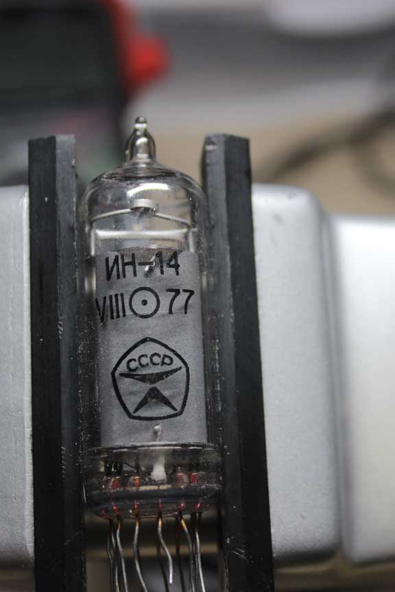
I chose to use an IN-14 Nixie tube for this task because of its warm, unique glow that never failed to capture attention. Also, Nixie tubes have a very interesting history of being used in old school scientific instruments and military equipment back before LCDs were a thing.
The particular tube I got (on eBay) was from Ukraine and according to the markings on the tube, made in 1977 in the Soviet Union. It even had the CCCP stamp of authenticity!
Testing the tube: 170 Volts!
The first order of business was to light this baby up to check that it is still indeed in working order after all these years and the shipping process.
To strike the tube, we need a high voltage of 170+ Volts to ionize the gas molecules. After this happens, the ions will be attracted towards the negatively charged number wire (cathode), and the resulting collision between said ions and said number wire will expel larger metal atoms. Electrons from the cathode itself are also attracted to the positively charged outside wire mesh (anode) and subsequently can collide and energize electrons from the expelled metal atoms. Upon collision, the electron in the metal atom gains energy and moves to a higher energy state and when it stabilizes and comes back down to the default energy state, that energy is converted to light. For a more detailed description, read this great article about how Nixie tubes work.
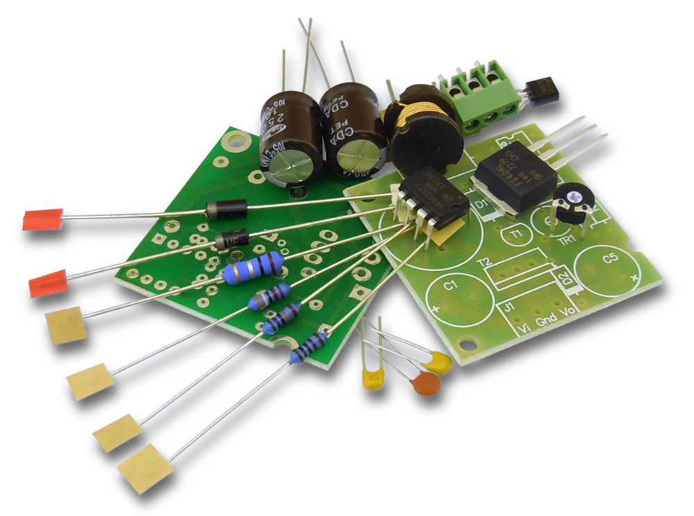
The first challenge was in obtaining 170+V, a non-trivial task. Linear bench power supplies usually don't go much past 50V, so I decided to go with a switching boost converter. In the future, I plan on building my own converter but in the interest of time, I used an existing kit that was readily available on eBay.
The kit came with a completely unpopulated board, the necessary passives and ICs, as well as clear instructions:
After about ~30 minutes of soldering, ensuring the orientation of the ICs were correct, I finished the assembly:
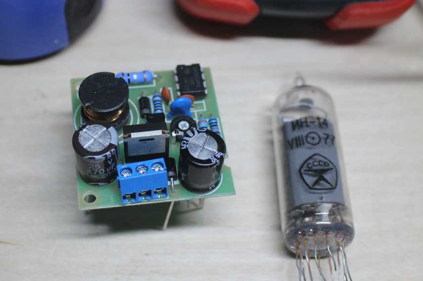
The converter took 10-18V DC and converted it to 110-180V DC set by a trim potentiometer. After 12V was fed to the converter and it passed the smoke test, I played with the pot, ensuring I saw 170V at the output.
Then, the moment of truth, time to give the tube some electricity. I used some nifty test hook probes to attach ground to the number "7" cathode and 170V to the anode WITH a 10k current limiting resistor in series like so:
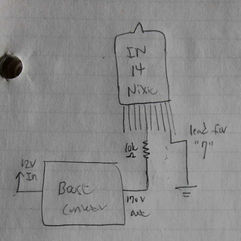
To figure out the value of CLR (current limiting resistor) you need, first look up the voltage drop across your Nixie when it's struck (for an IN-14, the relevant information can be found on this site). Since the typical maintaining voltage is 145V and supply voltage is 170V and we want 2.5 mA to flow through the tube (assume tube has very little resistance when struck) we can use the following relation to figure out the CLR value:
$$R=\frac{\Delta{V}}{I}=\frac{(170-145)\text{ Volts}}{\frac{2.5}{1000}\text{ Amps}} $$ $$= 10 \text{ k}\Omega$$
And... let there be light!
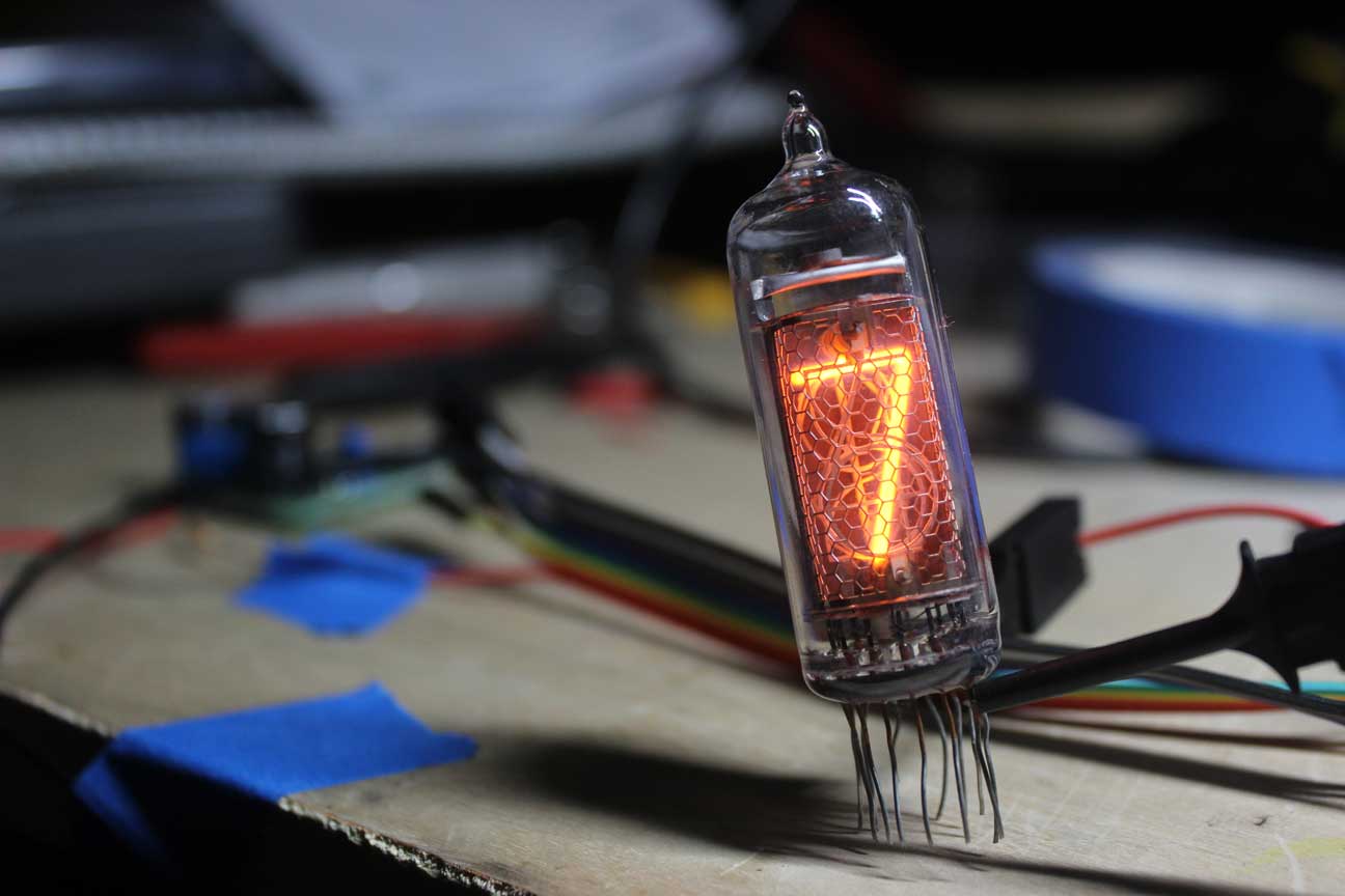
The picture doesn't really do the tube much justice, as the limited dynamic range of my camera doesn't capture the full glory and warmth of the tube's glow. It's just something you have to see for yourself.
Better Fixture for the Tube
Now that we confirmed the tube is working, we can start to prototype with it! However, attaching test probes for all 11 connections is a hassle, so we should use a breakout board. I looked around online for existing breakouts but there seemed to only be boards for IN-12 tubes. So, I set out to design my own with the following goals:
- Compatible with 0.1'' breadboard spacing
- Swap tubes without soldering, so need some kind of receptacle
- Current limiting resistor on board
After several iterations, I settled with the following design in Eagle CAD:
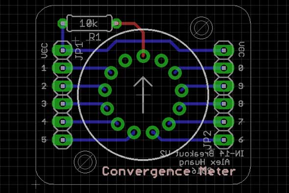
As expected, there was no library part for the IN-14 tube so I had to create that part myself. With the help of cmd-draw.ulp, I was able to get the pads in a circular pattern. Here's a video that shows how it's done.
The next tricky part was satisfying design goal 2: be able to swap out tubes easily. I had to order some tiny receptacles from Digi-Key as the parts were too specialized for eBay. To determine the dimensions we needed, I measured the Nixie tube pin diameter, which was 0.5 mm. Then, I looked for the receptacle with the greatest depth, which was about 1/8'' or 3mm. After ordering the receptacles and sending out the boards to Smart Prototyping, it was time to wait.
(I will put up the design files on Portfolio as soon as I sort out file hosting. For now, if you are interested in getting some of these boards just shoot me an email)
After about 10 days, my boards showed up:
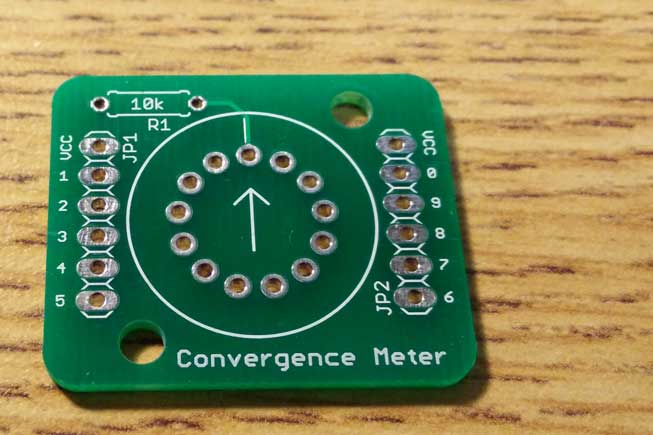
This was my first time using Smart Prototyping and for only $34 I was fairly impressed with the speed. The quality isn't as good as OSHPark but it shaved about 4-5 days from the turn time.
After populating the PCB and trimming+straightening the leads from the tubes, I got this:
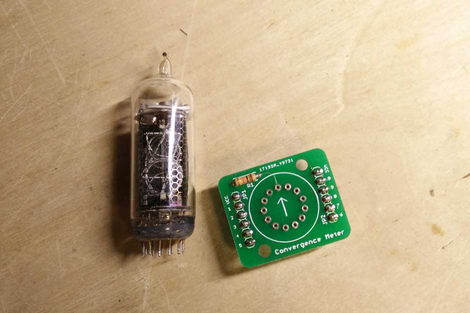
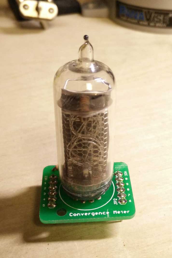
The tube sat firmly in the receptacles. You could dangle the whole thing upside down and the tube would not come loose. So far so good.
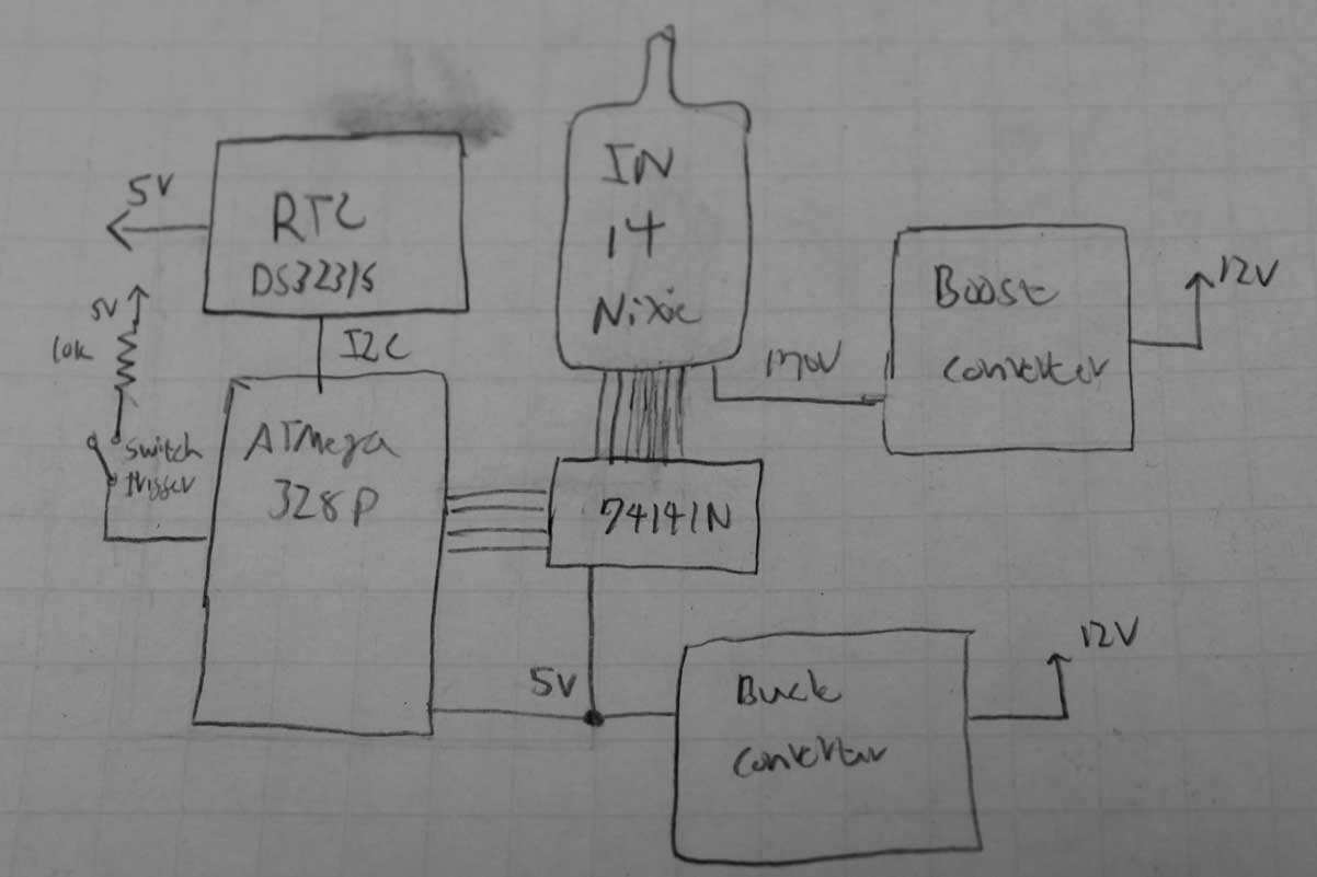
Microcontroller Time: Hardware
Now that we had the Nixie tube and its power source set up, we needed to give it some life by interfacing it with a microcontroller. For the purpose of getting this done quickly, I used the ATmega328p based Arduino Uno to prototype and will eventually use the standalone ATmega328p chip.
The diagram below shows the initial block design:
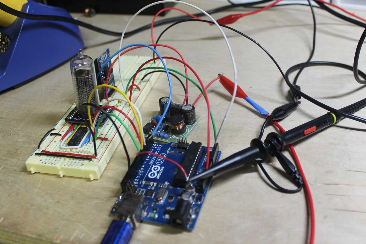
To prototype, we first build the circuit on a breadboard, then design a PCB after we confirm everything is working. Things to note:
- I won't be using the buck converter for the breadboard prototype as my bench power supply will be able to deliver 5V as well as 12V.
- The 74141 chip is out of production and hard to find nowadays. Instead, I will use a much more readily available K155ID1 Russian equivalent.
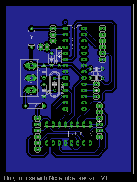
- The breakout board that will be used in the breadboard prototype is from the first design iteration, so it will appear different from the breakout seen above and the one used in the final product.
After a couple hours at the bench following the diagram, cutting wires, and soldering:
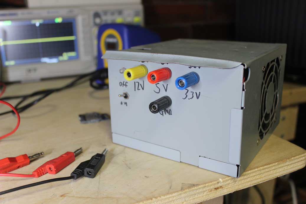
To get 5V and 12V, I used a bench supply that I built using a discarded PC ATX power supply:
Microcontroller Time: Software
In order to drive the tube in an interesting manner, we will have to play around with the software a little. Recall that at the very beginning, we set out the goal that Convergence Meter will be a 1 tube display for the amount of time that has passed since meeting your significant other/friend/someone important to you. The following goals will more specifically define how we want to display the time:
When triggered with a switch, the display should flash a sequence of numbers representing the days that have passed since meeting a person.
In its idle state (not triggered), the tube should display the current time's second's ones place. For example, if the time is 3:15:47 PM then the tube should display a 7. Additionally, in the idle state, the tube should fade between new numbers, so going from 6 to 7 would show 6 fading out while 7 simultaneously fading in. This functionality should be implemented using a timer interrupt PWM where the switching cycle is fast enough to fool the eye into thinking it's smooth fading. This approach leave our main loop plenty of time to do other tasks.
During the transition from idle to triggered, the meter should do something interesting. I have chosen a fading in and out of random numbers for the transition period.
Here is a software block diagram to show how the program should be structured:

The obvious constraint with this software design is that the interrupt has to be fast enough to fool the human eye into smoothing out the PWM of the tube, but leave enough time for the main loop to do its tasks. Therefore, I chose to have the switching period be 55 Hz, which should be plenty fast to fool the eye. The interrupt also had to be kept pretty lean in order to ensure that the main loop has time. As a result, the interrupt routine is partially written using direct port manipulation, which should save us a lot of cycles at the cost of readability.
I wrote the code according to the diagram above and added a line to flip the state of a pin every time the interrupt is called and checked the following on the oscilloscope:
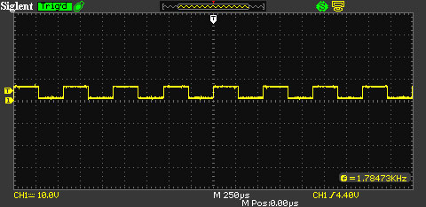
This translates to an interrupt frequency of \( 2 \cdot 1.785 = 3.57 \text{ kHz}\) (the factor of 2 comes from the fact that the frequency on the scope is comprised of 2 interrupt calls). To figure out the switching frequency, we simply take into account of the number of brightness levels we have. So for 64 brightness levels:
$$ 3.57 \text{ kHz} \cdot \frac{\text{switch cycle}}{64 \text{ brightness levels}} $$
$$ \approx 55 \frac{\text{switch cycle}}{\text{second}}$$
Which is plenty fast for fading our Nixie tube.
The full code can be found at github. I've gone ahead and included plenty of comments so it should be straightforward to follow.
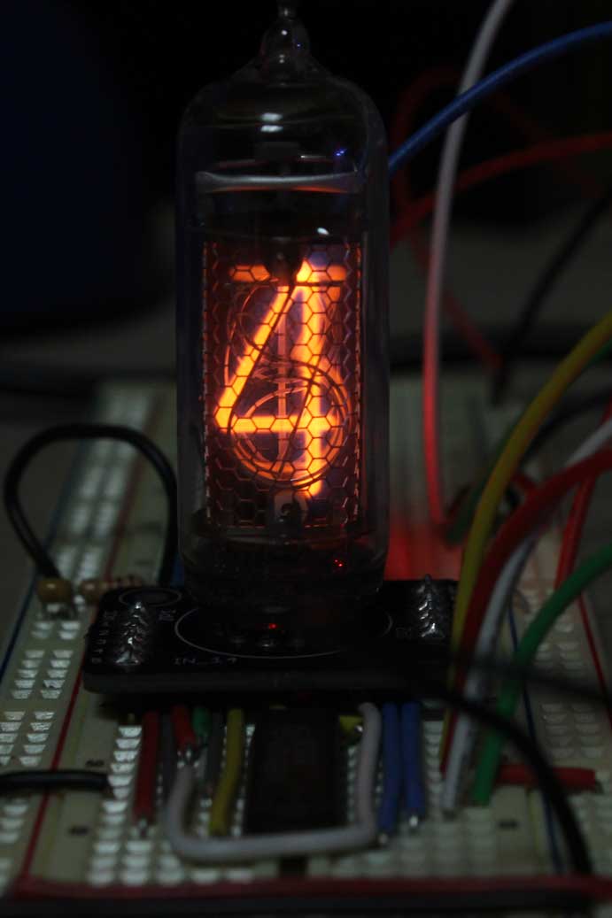
After uploading to the Uno and debugging, I got the Uno talking to the RTC and manipulating the K155ID1, fading the Nixie in and out. Here is a picture of the tube fading from a 3 to a 4:
Something More Permanent: PCB
Now that the prototype is completed and we have successfully implemented the required functionality in hardware and software, it is time to move on from the breadboard prototype to something more suited for production: a PCB.
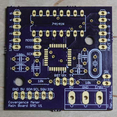
Using the same schematic as the one we used to build the breadboard, I created a PCB that featured the Uno's microcontroller along with everything else from the breadboard prototype:

and after some work with placing/routing the board:
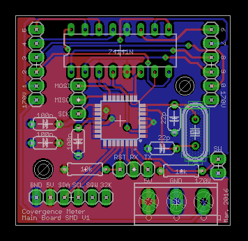
I focused on reducing board size as that decreased cost of production. The routing for the 74141N/K155ID1 was pretty tricky. I could have used SMD resistors and capacitors but since I have access to through hole passives for free from the MIT EE lab, I chose to use those.
For this board run, I sent it out to OSHPark as I didn't need that many copies and it would be less than 4$ per board for an order of 3.
While waiting for the miniature board to arrive, I also created a single sided version of the board for fun/self etching. I was pretty proud of the fact that I got the board routed without using any jumper wires:
Since space wasn't a constraint for the single sided run, I went with the through hole ATmega328P chip. I etched the board and soldered the components and it came out pretty well, but the boards from OSHPark showed up before I had time to test the single sided boards.
Here are the boards from OSHPark:
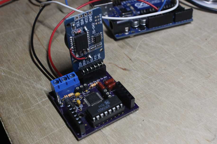
The board was tested and proved to work. The next step was to put everything we had built into a nice package.
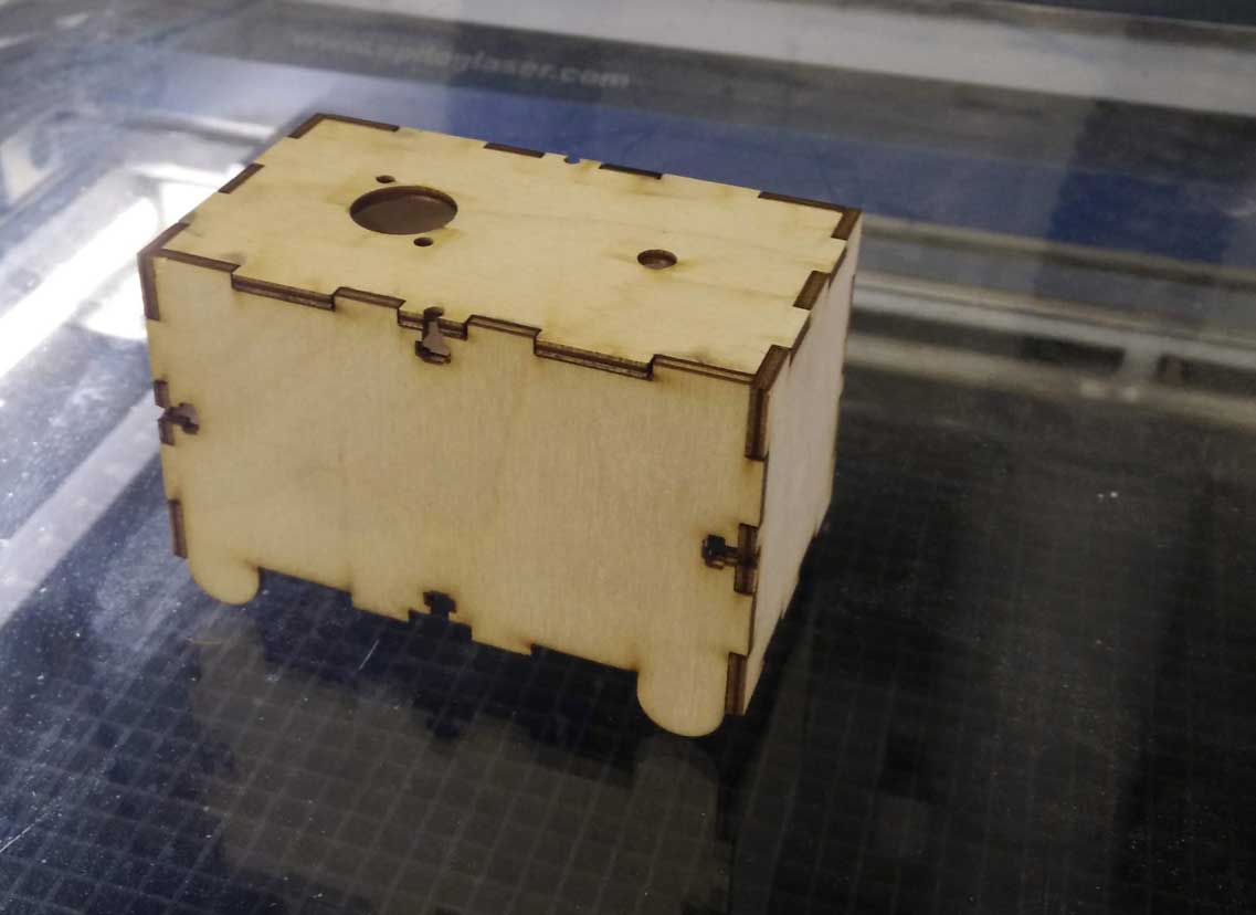
Enclosure Design
To enclose everything, I chose to build a box out of laser cut 1/8'' plywood. The main concern with the enclosure is that it has to be stable enough for the user to be able to press the button without tipping, so the longest dimension of the box should not be in the vertical plane.
I did a rough layout of the various components (buck converter, main board, boost converter) and measured roughly how wide/deep the box would have to be. The height was estimated by inspection, mostly to give enough clearance for the wires that I would run from the switch and nixie tube to the breakout board.
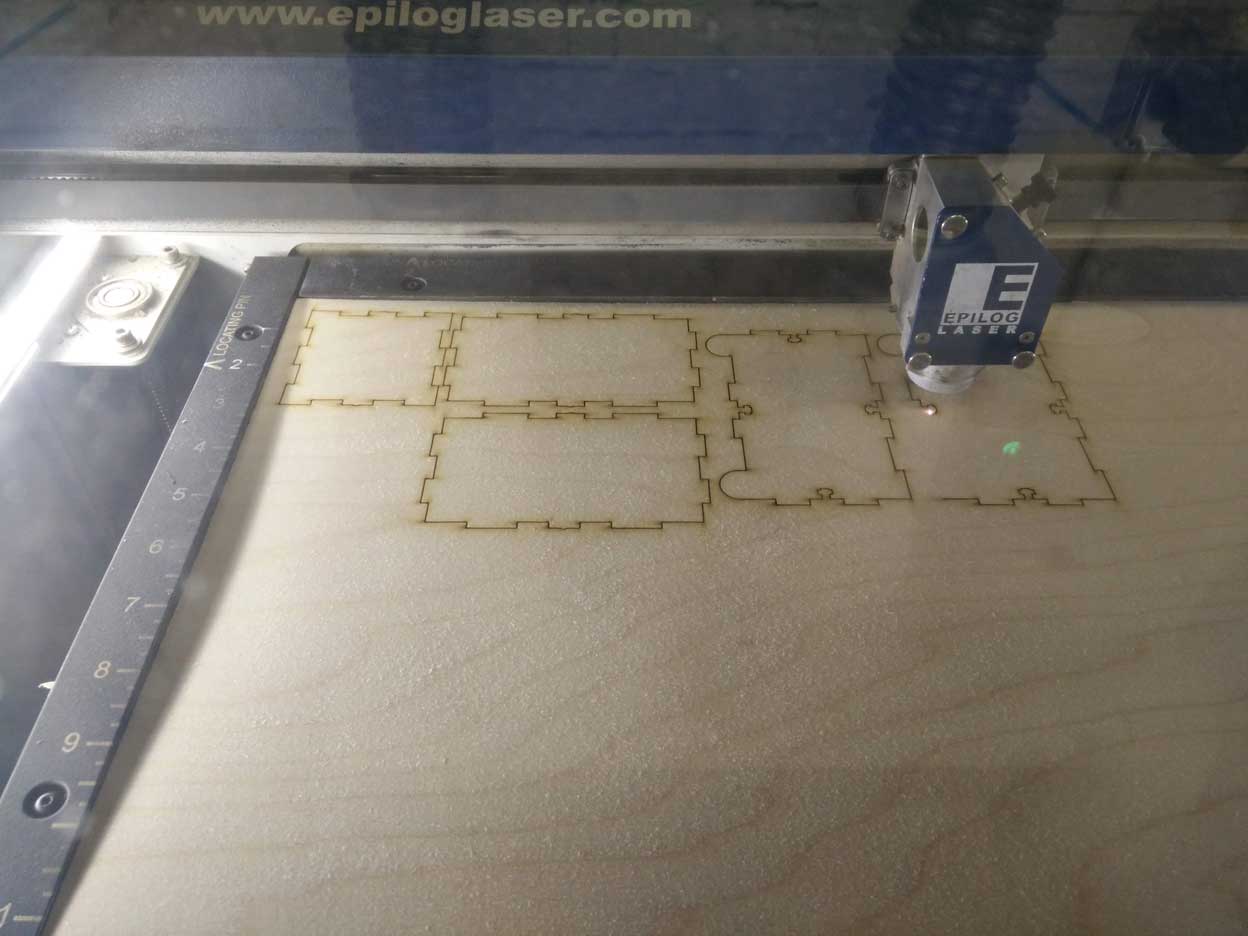
With the help of MakerCase, I got an SVG file for the sides of the finger joint box after I inputted the required dimensions. To complete the design, I converted the SVG into a DXF file, imported that into Autodesk inventor, added some T-slots (note you can add t-slots on MakerCase but the settings menu was not flexible enough to generate exactly what I wanted), and incorporated the necessary mounting holes for the switch, tube, and 12V barrel connector.
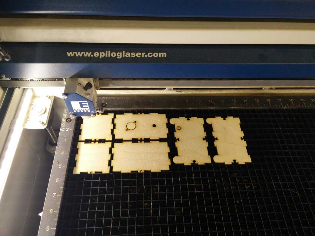
Then, I exported the drawing from Inventor as a DXF and fed it over to the MIT Hobby Shop laser cutter. This is the result:
Putting it all together
At this point, we have all the necessary pieces to complete the project and it is a matter of assembly. First, I tried fitting the electronics without any tape/wires:
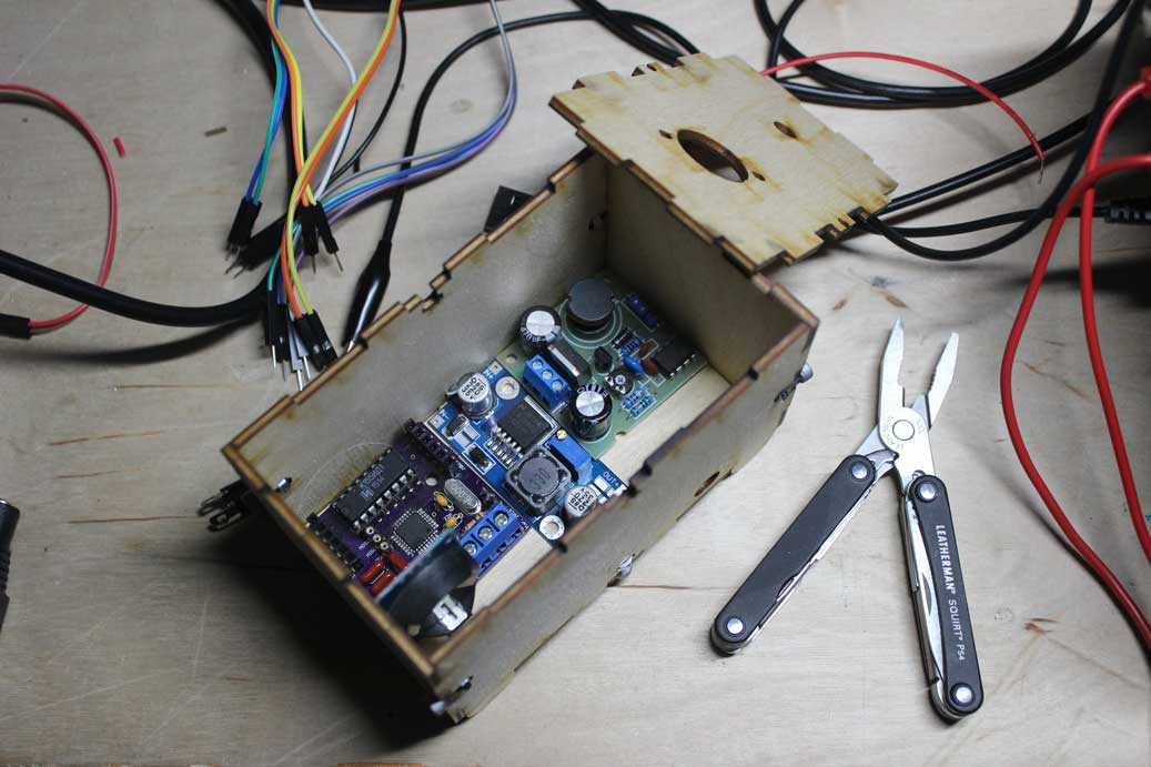
The fit was pretty much expected. so it was time to put in the tube, switch, and wiring and throw some double sided tape on the PCBs to keep them from rattling around.
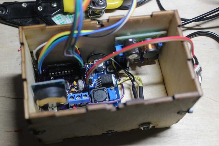
I ended up modifying the configuration a little bit to give the wires coming from the 12V barrel connector a little more room, but everything fit nicely.
Upon first closing the lid and powering up the meter, I noticed that the hardware interrupt service would be triggered at random times. After debugging, I noticed the problem would go away when I removed the wires coming from the switch, so they must have been picking up some EMI from the boost converter's inductor switching at high frequency. This is a somewhat hacky solution, but I ended up wrapping the wires in aluminum foil and putting a thick sheet of folded foil insulated with electrical tape between the boost converter and the wire leads for shielding:
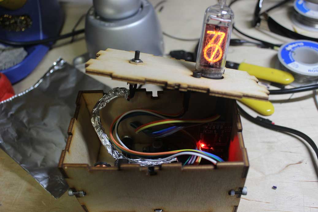
The problem was solved, although it was cool to see convergence triggering at random times. It might be something to consider implementing in software at a later time!